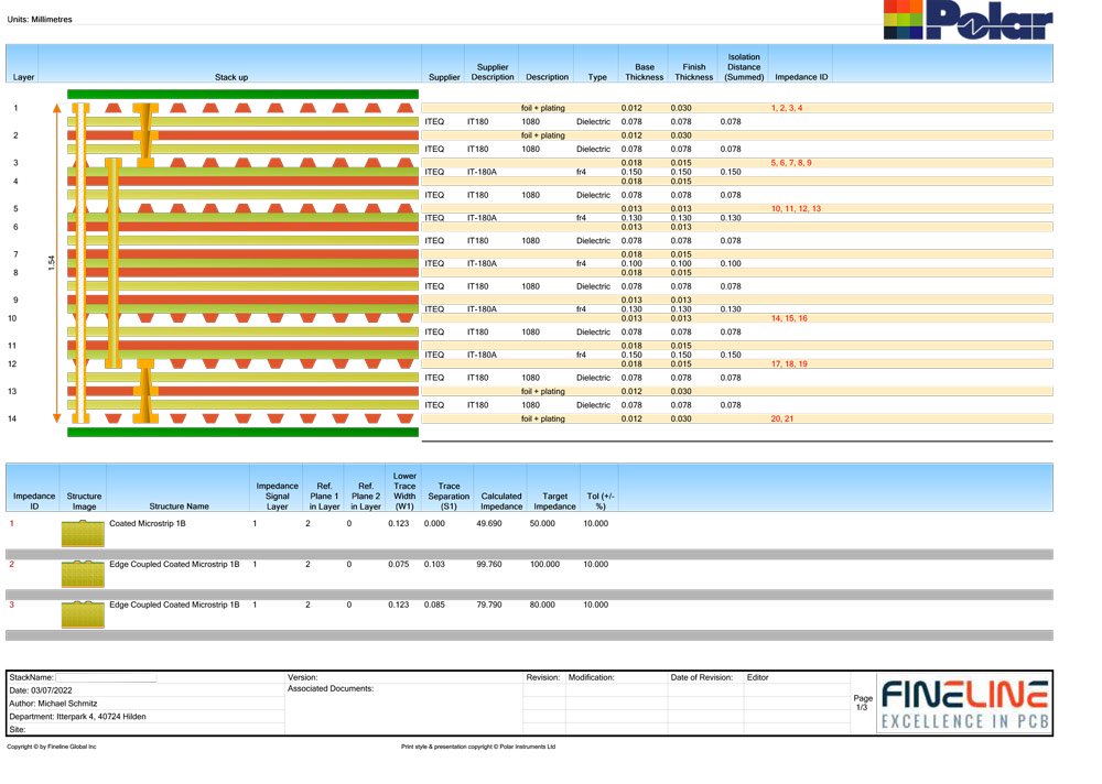
With higher signal switching speeds, short transition times and high clock rates, today’s printed circuit boards require designs that are tailored to suit each individual application.
The interaction of track/gap, dielectric thickness, dielectric constant of the insulating material and track thickness must all be balanced to ensure a design can be manufactured, with good yields, which meets designers’ requirements and expectations.
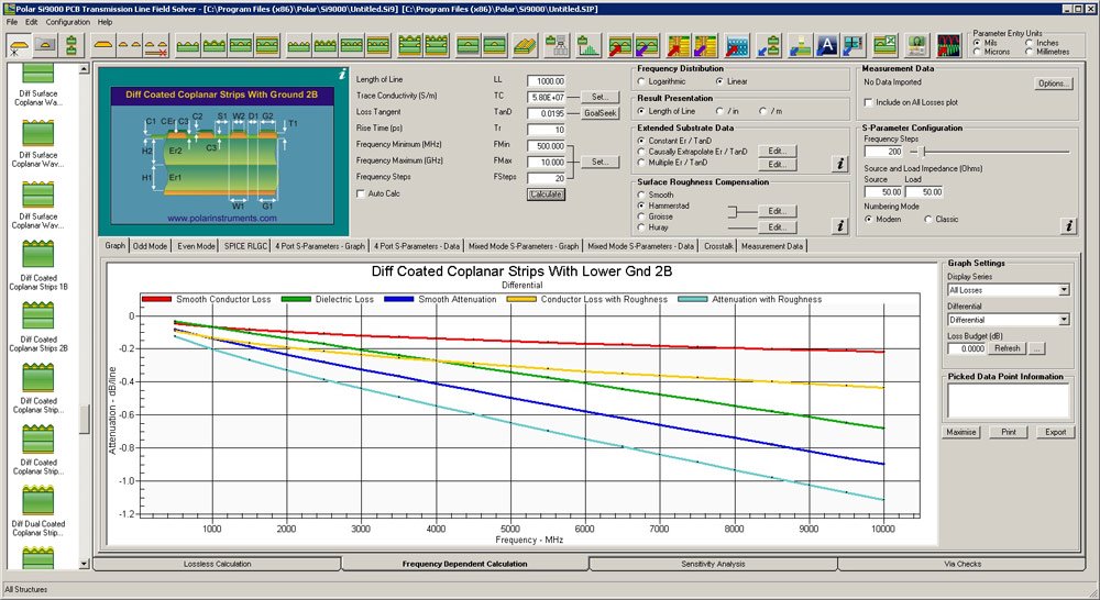
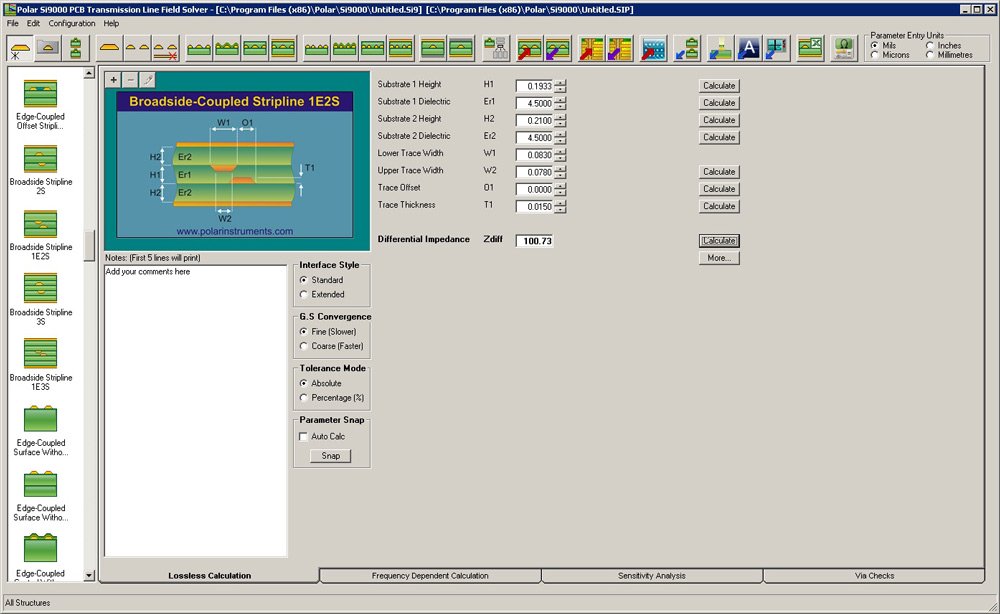
Need a controlled impedance PCB? Fineline have the right tools for your design. With our Polar software we accurately model the correct layer structure(s) and calculate the optimal PCB features to yield the required target impedance value(s). With over 130 different impedance models available for this and an extensive materials library, you can be sure that the optimal solution is realised, at the best cost.
Prior to manufacture, the theoretical structure(s) are modelled against predicted process values and calculated impedances compared against design requirements. Minor changes can be made to track/gap and/or dielectric separations to ensure that the manufactured PCB yields values as close to nominal as possible, giving the designer peace of mind that the finished PCB meets specification.
The interaction of track/gap, dielectric thickness, dielectric constant of the insulating material and track thickness must all be balanced to ensure a design can be manufactured, with good yields, which meets designers’ requirements and expectations.
Need a controlled impedance PCB? Fineline have the right tools for your design. With our Polar software we accurately model the correct layer structure(s) and calculate the optimal PCB features to yield the required target impedance value(s). With over 130 different impedance models available for this and an extensive materials library, you can be sure that the optimal solution is realised, at the best cost.
Prior to manufacture, the theoretical structure(s) are modelled against predicted process values and calculated impedances compared against design requirements. Minor changes can be made to track/gap and/or dielectric separations to ensure that the manufactured PCB yields values as close to nominal as possible, giving the designer peace of mind that the finished PCB meets specification.
Every developer who deals with the subject of impedances should know the PCB influencing variables on the trace impedance. This is true even when working with field solver programs such as Polar Instruments Si8000/Si9000 Advanced Software.
Read our presentation here to learn more.
Read our presentation here to learn more.


