PCB MANUFACTURING PROCESS - FINELINE GLOBAL

A comprehensive guide to our PCB manufacturing process

1.0

DESIGN REVIEW AND PREPARATION OF PRODUCTION TOOLS.

The first stage in the PCB manufacturing process involves a review of the manufacturing data package that is provided by the designer and preparation of the manufacturing tools and CAM data.

1.1

Production data package

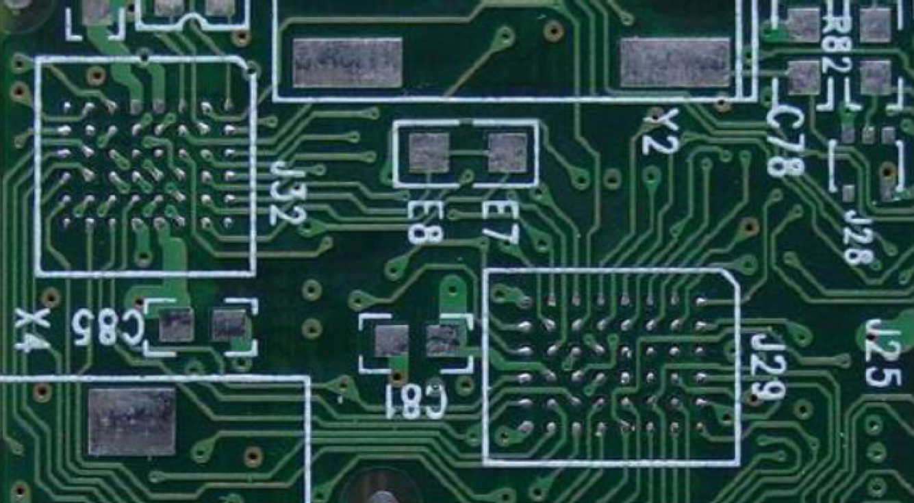
The output of the PCB fabrication process design is a data package provided to the manufacturer in an industry standard format – Extended Gerber or ODB++. The Gerber files define the copper layers, solder mask layers, component notations. In addition, the manufacturing data package includes a drill file, netlist and general specifications.

1.2

Design for Manufacturing

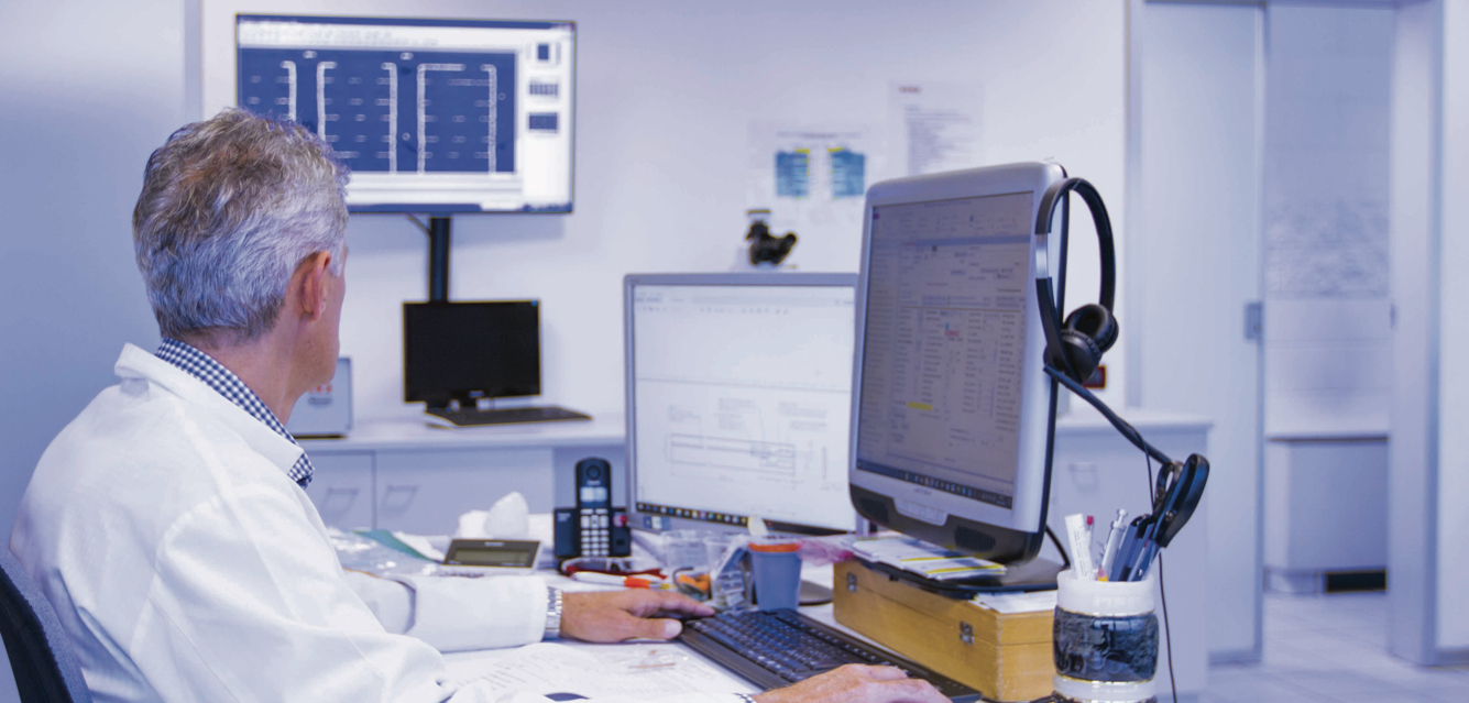
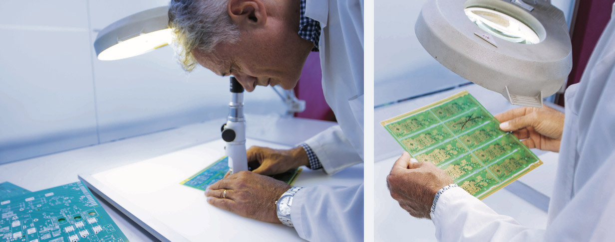
Engineering will check the data package and verify that all the information needed for manufacturing is clear and complete. We'll also check that the design and specifications match the manufacturing capabilities.

1.3

Once all the engineering questions have been resolved the necessary tools for production will be prepared.

1.31

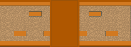
Preparation of the manufacturing panels.

Manufacturers use standard manufacturing panels. The manufacturing panel has to be designed to maximize material usage, considering the PCB dimensions and manufacturing requirements: process control coupons, tooling holes and handling.

PCB production panel chart
1.32

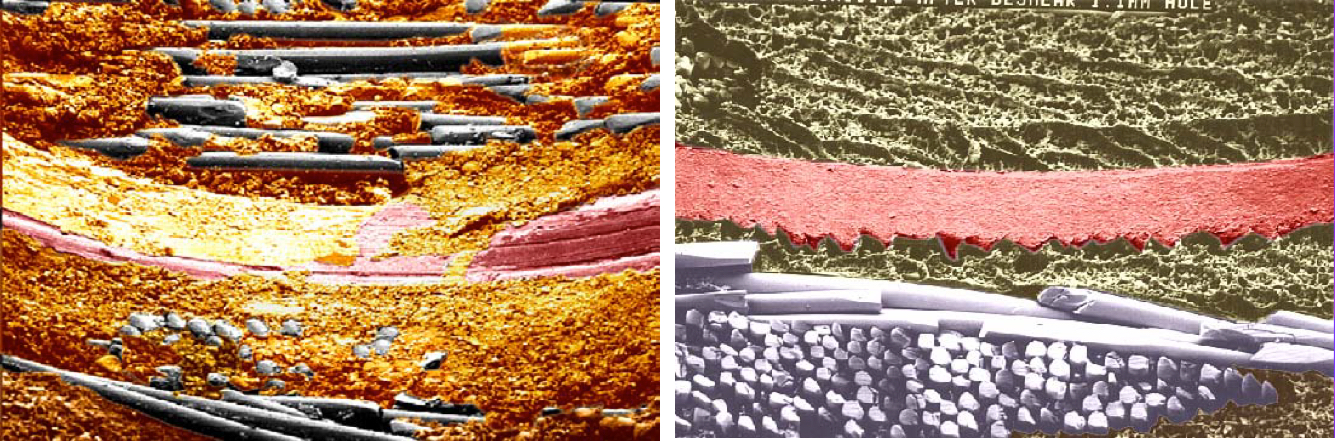
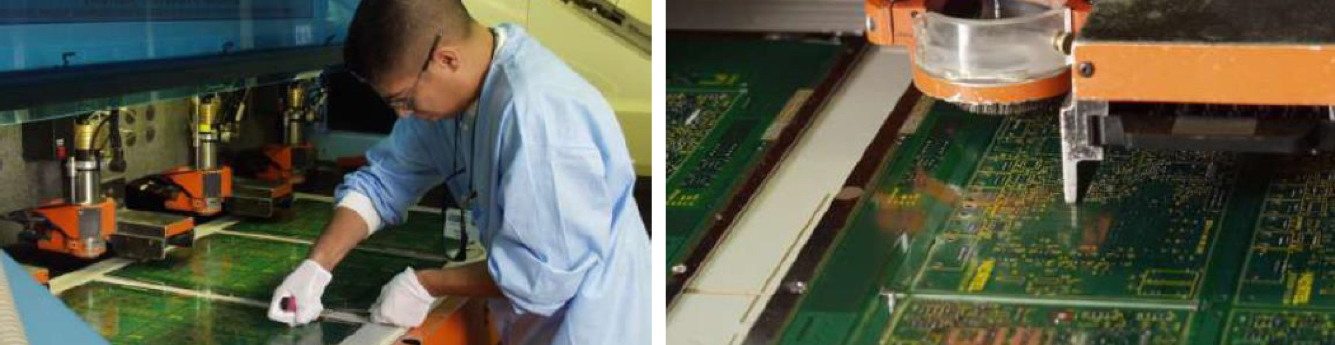
Working film (photo tools) preparation.

Using a laser plotter, a film is created for each PCB assembler layer boards. The laser plotter is in a temperature and humidity controlled dark room. The films are registered with each other to assure perfect alignment between the layers.

The punched registry holes are used later to align the films in the UV exposure process. Another method is using laser direct imaging (LDI), using a CCD camera in the exposure machine in order to register the phototool.

PCB Brushing and Desmearing chart
2.0

Inner Layers

In preparation of the inner layers, we take a base material of an epoxy resin and glass fabric, coated on both sides with copper foil and remove the excess copper, to leave copper traces only where we need them in order to realize the electric circuitry.

2.1

Base Material

The core of the inner layer consists of epoxy resin and a glass fiber fabric which is coated on both sides with thin a layer of copper foil. In most cases FR4 material is used.

The copper clad on both sides is cleaned by a chemical cleaning process for inner layers to remove oxides and possible contaminations. Simultaneously, the rotating brush rollers roughen the copper surface to ensure sufficient mechanical adhesion.

PCB base material scheme
2.2

Dry film lamination

The core material is passed through a heated roller pair (Temperature: approximately 110º C Pressure: 3-5 BAR). The Cu surface becomes sensitive to UV light and, therefore, further processing is done in yellow light area only.

PCB dray film lamination
2.3

Exposure on inner layers

The film for the layer is placed on the laminated material and the laminate layer is exposed to an energy-rich UV lamp. The traces of the PCB are transparent in the film and the underlying laminate in exposed to the UV light. The exposed are will be chemically polymerized and the traces will harden.

The area which is covered by the black part of the film will not polymerize and can be washed away in the development process.

PCB layers scheme after exposure
2.4

Development process

The development is done by spraying the inner layers horizontally with a Sodium Carbonate solution and subsequently rinsing them with fresh water and drying them. The unexposed areas are now removed.

PCB after development process
2.5

Etching of inner layer core

The inner goes through another process of spraying, rinsing and drying. This time with an acid solution. This process removes the copper from the exposed area, leaving copper only in the traces and pads.

The copper thickness of the layers will determine the speed of the process. Thicker copper layers limit the fineness of the conductive pattern.

A PCB after etching scheme
2.6

Stripping

The lacquer layer is removed by passing the material through a Caustic Soda solution

PCB after striping process scheme
2.7

Automatic Optical Inspection (AOI)

Inner layers undergo an automated optical inspection to detect opens and short as well as proper circuit geometrics in comparison with the original design data.

2.8

Braun Oxide Preparation

The inner layers go through a chemical surface preparation process to roughen the surface and improve the adhesion between the PREPREG resin and the copper surface in the lamination process.

3.0

LAMINATION

3.1

Material Layup

The layers are stacked up before lamination. Starting with a copper foil at the bottom (that will be used to build the bottom outer layer). On top of the copper layer PREPREG layers, on top of the PREPREG the inner layers are placed, separated by PREPREG layers and on top of the inner layers, PREPREG layers and a second copper foil (that will be used to build the top outer layer).

PREPREG is a partially cured epoxy resin with glass fiber, polymerized by the PREGREG manufacturer. It is used as the insulating material and adhesive between the layers of the PCB components.

PCB stack-up layers chart
3.2

High Pressure Lamination

The stacked up layers are laminated under a vacuum, high temperature and high pressure press. Multiple PCBs, separated by dividers are pressed simultaneously. The heat and pressure melts and hardens the epoxy resin in the PREPREG, while the pressure fuses the printed circuit board.

high pressure machines
3.3

Trimming

The Flash (material hanging out of the laminated panel are routed off, leaving a clean panel that looks like a piece of laminate.

4.0

DRILLING

4.1

X-RAY analysis

As a preparatory stage, the invisible pads in the inner layers are identified using X-RAY. The X-Ray analysis allows to detect the pads and to calculate new reference holes for the drilling.

PCB X-RAY analysis chart
4.2

Drilling

The PCB is done on a high speed CNC drilling machine (up to 280,000 revolutions/minute). Drilled holes must be clean and smooth as possible to enable quality copper plating of the holes. Optionally, up to 3 panels are stacked up and drilled simultaneously.

The panels are placed between a based plate and top aluminum sheet. The base plate prevents drilling into the drill machine and allows the drilling deeper than the panel, avoiding burrs. The aluminum top plate avoids burrs and prevents the drill from deflecting. Both plates protect the surfaces of the panel from damage and scratches.

4.3

Brushing and Desmearing

After the drilling the surface of the PCB is mechanically brushed using an oscillating and rotating brush rollers. The drilled holes are cleaned with a permanganate solution or oxygen plasma in order to remove resin that may have smeared on the copper. Resin residues on the copper may prevent proper electrical conductivity between the hole plating and the traces in the layers.

5.0

ELECTROLESS PLATING

5.1

Electroless Plating

In order to create an electrical connection between the drilled holes and all the layers, a conductive film, about 0.5-0.7 micron thick, is produced by chemical copper. This conductive layer is the basis for copper plate process applied later.

PCB electroless plating
6.0

OUTER LAYERS AND PLATING

This process is similar to the process employed in constructing the inner layers. The difference is that in this step we plate the holes and the traces and pads of the outer layers using an electrolytic copper plating process.

6.1

Dry Film Lamination of outer layers

This process corresponds to the process employed in the inner layers. The panel is passed through a heated roller pair (Temperature: approximately 110º C Pressure: 3-5 BAR). The Cu surface becomes sensitive to UV light and, therefore, further processing is done in yellow light area only.

6.2

Exposure and Development

This process corresponds to the process in the inner layers. However, in this process a negative exposure process is used. The conductive wires are not covered by the resist and can be galvanised by copper plating. The areas between the conductive traces are covered with polymerised laminate.

6.3

Electrolytic Copper Plating

All traces and holes are coated with a conductive electro-deposited copper layer. The holes create the electric connection between the conductors on layers and a good connections require a 20-25 micron of copper on the walls of the hole. The overall copper thickness on the outer layers is determined, therefore by the copper thickness of the material and the additional 25-30 microns added in the plating process.

PCB after copper plating scheme
6.4

Tin Plating

A second plating process is performed to protect the copper conductors during the etch process that will follow, therefore the layer is also often indicated as etch resist.

PCB after copper plating process scheme
6.5

Outer Layer Dry Film Stripping

The dry film is removed to expose the copper layer for etching.

6.6

Etching and Tin Stripping

An etching process is performed to remove the excess copper, leaving copper only in the traces and pads that are protected by the tin plating. Then, the tin is removed using nitric acid.

7.0

SOLDER MASK

Solder mask is applied to most printed circuit boards to protect the copper surface that will not be protected by soldering in the assembly process and to prevent solder shorts during assembly.

7.1

Panel are brushed and cleaned.

7.2

The panel is coated on both sides with an epoxy solder mask ink 15-25 microns thick.

7.3

Using a UV printer and a photo-tool film, the solder mask is hardened on the area where we want the solder mask to remain.

7.4

The panels are processed through a developer that strips off the solder mask from the areas that should be exposed.

7.5

The solder masked is further hardened in an oven.

PCB solder mask process scheme
8.0

SURFACE FINISH

The surface finish applied a solderable surface finish to the copper surfaces that are not covered by solder mask. This finish protects the copper until the components are assembled and soldered to the printed circuit boards. Several surface finishes are available. The most commonly used are Hot Air Leveling (HAL) and Electroless Nickel Immersion Gold (ENIG).

8.1

HAL

The HAL process creates a solder on all pads. The entire panel is immersed in liquid solder and is removed from the solder through hot compressed air. Excess solder (which did not bind with exposed copper) is blown away and the copper pads and holes are left plated.

The solder material used in the process is either Tin"Lead alloy or Tin only(Lead Free).

8.2

ENIG

In this nickel is chemically deposited over the copper and then a thin layer of Gold in deposited over the nickel. The entire process is automated, moving the panels through a series of tanks, cleaning the copper, depositing a 3-5 micron layer of nickel and a layer of gold of minimum 0.05 micron.

8.3

Hard Gold Plating

Edge connectors are electroplated with 1-1.5 microns of gold over 4-5 microns of plated nickel. This type of plating in cases where the plating needs to withstand the erosion of multiple insertions.

9.0

LEGEND PRINT

Legend is printed onto the PCB using a screen printer.

legend print on a PCB
10

ROUTING

Using a CNC the manufacturing panels are cut out into individual PCBs and PCBs are routed into their shape according to the design data.

PCB routing process
11

ELECTRICAL TEST

Each PCB is electrically tested against the design data using a "bed of nails" adapter or a flying probe tester.

Fineline QA manager checks PCB reports
12

FINAL QUALITY CONTROL

This is the final inspection of the finished PCB product. It checks for any cosmetic defects such as scratches and impurities, using IPC600 as a reference.

Fineline QA manager examining a panel with x-out

Knowledge Centre

Embedded Resistors in Printed Circuits: Fineline Global Commitment to Innovation and Advancing Technology

Embedded Resistors in Printed Circuits: Fineline Global Commitment to Innovation and Advancing Technology

By: Maysa Salameh, Chief Technology Officer, Fineline Global

Explore more
Multilayers: Design Rules

Multilayers: Design Rules

Explore more
Surface Finishing – Advantages & Disadvantages

Surface Finishing – Advantages & Disadvantages

Advantages & Disadvantages

Explore more
Embedded Resistors / Capacitors Technology

Embedded Resistors / Capacitors Technology

All about embedded resistors and capacitors technology

Explore more
Stacked or Staggered Microvia

Stacked or Staggered Microvia

Helping you pick the right microvia for your design

Explore more
Rigid-Flex PCB

Rigid-Flex PCB

The advantages and materials of Rigid-Flex PCBs

Explore more
Efficient Heat Dissipation

Efficient Heat Dissipation

Understand efficient heat dissipation in PCBs

Explore more
Back Drill Technology

Back Drill Technology

The Advantages and uses of Backdrill Technology

Explore more
Optimised PCB Design – Design Rules In Your Layout System

Optimised PCB Design – Design Rules In Your Layout System

Explore more

We're here to help

 From engineering advice to selecting the right manufacturing partner for
you – our experience and expertise gives you the right solution. 

Get in touch and let’s start working together.